
The Invisible Machine Behind Every Chip in Your Phone: How EUV Lithography Works and Why Only One Company Makes It
ASML's extreme ultraviolet lithography machines operate in conditions more extreme than the surface of the sun, use light that cannot travel through air, and remain the only technology capable of producing the world's most advanced chips.
DURMUS EFE KOCH
5/21/20262 min read

Inside every modern smartphone, laptop, and AI system are chips containing billions of transistors etched onto silicon wafers at scales measured in nanometers, roughly the size of a few atoms. The machines that make this possible operate under conditions so extreme that they represent one of the most complex engineering achievements in human history. At the center of this process is extreme ultraviolet (EUV) lithography, a technology developed over decades by Dutch company ASML, which today holds a global monopoly on its production.
Light That Cannot Travel Through Air
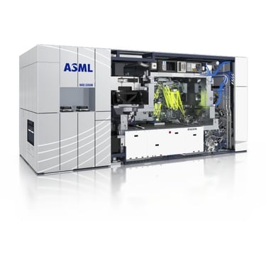
EUV lithography uses light with a wavelength of just 13.5 nanometers — approximately fourteen times shorter than the 193-nanometer light used in the previous generation of chip-making equipment. At this wavelength, EUV light is absorbed by virtually every material, including air itself. For this reason, the entire machine operates in a vacuum, and the optical system uses ultra-precise mirrors rather than lenses, since no material can properly focus EUV light the way conventional optics can.
To generate EUV light, the machine fires a powerful CO2 laser at a continuous stream of tiny molten tin droplets. The laser vaporizes each droplet, creating a plasma that is hotter than the surface of the sun and emits EUV light. Precision optics, manufactured by Germany's Carl Zeiss, then capture and direct this light to print circuit patterns onto silicon wafers.
ASML's 2026 Breakthrough and the High-NA Era
In February 2026, ASML announced a major advance in its EUV technology: increasing the power of the light source to 1,000 watts, up from 600 watts in current machines. This improvement is expected to raise chip production throughput to approximately 330 silicon wafers per hour by 2030, compared with 220 today — a 50% increase. The company achieved this by doubling the number of tin droplets to roughly 100,000 per second and using two smaller laser beams to shape each droplet.
The company's next-generation platform, known as High-NA EUV, entered commercial use in 2025–2026. These machines, designated the EXE:5000 and EXE:5200B, cost approximately $380 million each and are the size of double-decker buses. They improve resolution to 8 nanometers, enabling chipmakers to produce transistors 1.7 times smaller and achieve transistor densities 2.9 times higher than standard EUV. Intel has been the most aggressive early adopter, deploying the High-NA EXE:5200B for its Intel 14A process node. ASML reported Q1 2026 revenue of €8.8 billion and raised its full-year guidance to between €36 and €40 billion.
Why Only a Handful of Companies on Earth Can Make These Machines
ASML's EUV systems represent the culmination of decades of development and multi-billion-dollar investment in technology that competitors repeatedly deemed too difficult and too expensive to pursue. Today, TSMC, Samsung, and Intel are the only chipmakers deploying EUV at scale, and ASML remains the sole supplier. EUV systems have never been sold to China, blocked since 2019 under U.S. export pressure. In December 2025, Reuters reported that China had secretly completed a prototype EUV system in Shenzhen, though working chip production from that device is not expected before 2028–2030.
References
ASML. (2026). EUV lithography systems. https://www.asml.com/en/products/euv-lithography-systems
Techzine. (2026, February 23). ASML achieves EUV breakthrough: 50 percent more chips in the foreseeable future. https://www.techzine.eu/news/infrastructure/139010/asml-achieves-euv-breakthrough-50-percent-more-chips-in-the-foreseeable-future/
Tom's Hardware. (2026). ASML's roadmap for chipmaking lithography tools examined. https://www.tomshardware.com/tech-industry/semiconductors/asml-lithograpy-roadmap-examined-from-duv-to-hyper-na
Wikipedia. (2025). Extreme ultraviolet lithography. https://en.wikipedia.org/wiki/Extreme_ultraviolet_lithography